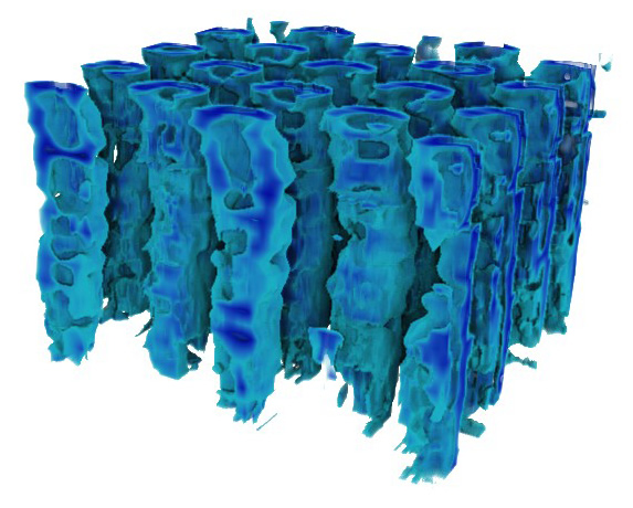
As advanced Semiconductor devices become increasingly complex in the 3rd-dimension, there is increasingly the need to be able to measure and inspect a vertical cross section through the device.
This can currently be achieved, using either a cross-section scanning electron microscope or a transmission electron microscope. Here a Focused Ion Beam, FIB, system is typically used to create the device cross section. In the case of TEM, additional steps are needed to create an electron transparent, lamella of the device. This sample preparation is both time consuming, expensive, and may be coupled with added complication of damaging ions being implanted into the sample surface.
The RPM can perform 3D tomography in-situ on the wafer, by application of a hard probe for atomic layer removal, ALR, and a bespoke probe for either height measurement of current measurement. This switching between probes is automated with a co-localised positioning of the probes for efficiency and ease of use. As a result a sequence of steps; ALR followed by measurement enable a 3D tomographic cross section of the device to be produced. The automated nature of this process means a 3D section can be achieved in minutes rather than hours, the result is fast cycle times without the need to scrap the wafer.


