
Thin film deposition processes deposit a wide range of materials in the chip fabrication process and can involve a variety of different techniques. The most common are chemical vapour deposition, CVD, physical vapour deposition, PVD, epitaxial deposition, and more recently, atomic Layer deposition, ALD. New techniques, such as selective deposition, where the film is only deposited on certain areas of the device, and the deposition of new materials, such as Ruthenium are important for future devices.
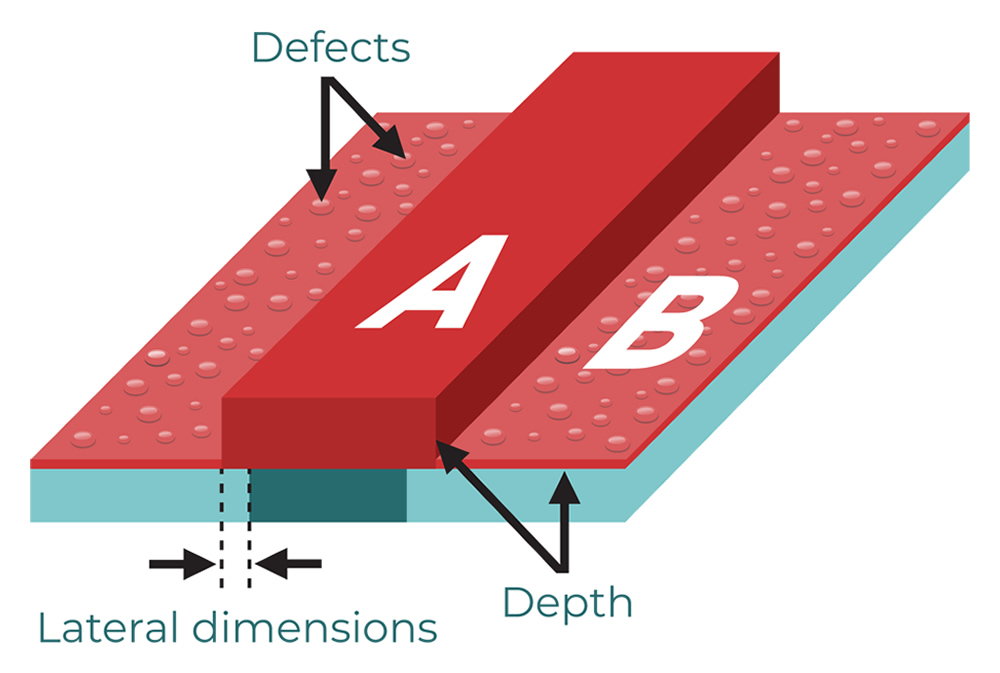
A variety of metrology techniques are used to measure a deposited films properties, including film thickness and uniformity, step coverage, surface roughness, film composition, and defect density.
As these films have become thinner, and the topography on which the thin film is deposited more complex it has become increasingly difficult for optical and e-beam techniques to provide the required metrology information. The ability of the RPM to detect small defects, measure the grain size of deposited metals and the change in step height resulting from selective deposition make it a valuable addition in the development and characterisation of new deposition processes. As these processes are introduced into production for future generation devices, the RPM can enable in-line defect monitoring..