Etching is the process of transferring the Litho pattern into the wafer by selectively removing those areas not protected by the resist. The etch process used for advanced semiconductors is usually plasma or reactive ion etching.
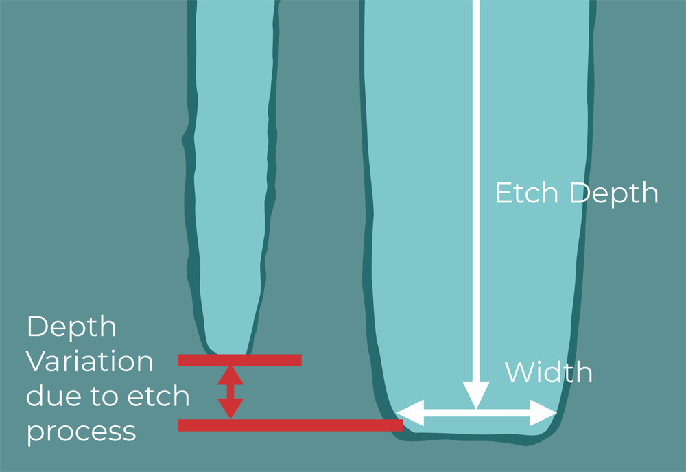
The rate that material is removed or ‘etched’ from the wafer can differ across the wafer due to variations in the gas flow, it can also vary within a device due to differences in the size of features and pattern density.
It is critical in etching processes to ensure that the correct depth is achieved to guarantee correct device functionality. Under etching can result in device failure, over etching can damage or remove the underlying film causing device performance issues or failure. Therefore, metrology techniques which can accurately and reliably measure depth on the nano scale are required.
E-beam techniques do not accurately measure structure depth and optical metrology is constrained to measuring large targets outside of the device, so cannot detect local variation in etch depth e.g. from pattern loading effects.
In this application, the RPM delivers benefits which these other tools cannot. Etch depth is measured with an accuracy typically of 0.5nm 3 sigma, over a wide range of etch depths and feature sizes. This then enables the etch process to be both optimised and controlled effectively.